
The MSP430F5529 is a low power mixed signal microcontroller. This is what it looks like.

It is an 80 pin IC that we can use in any of our applications. The datasheet (linked here) is of this 80 pin IC and everything written in it assumes you’ve this soldered to a board and ready to use with all the necessary components and power supply.
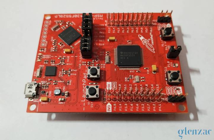
In this tutorial series we’ll be using the MSP430F5529LP which is the LaunchPad Boards from TI. These LaunchPad boards contain the specific IC and all the necessary components, GPIO headers, buttons, LEDs and everything else that you’ll required to program and debug your applications on it.
So the LaunchPad board helps you to build and test your application on the MSP430F5529. They are only to help you better understand the MSP430 series boards, their architecture and how the different peripherals work.
Now, let’s imagine that your ultimate requirement is to make a device that periodically measures ocean temperatures and currents (not the flow of electrons but the ocean current 🌊 ). So you go out and drop this device on the ocean floor in a special capsule or something. You are trying to log oceanic data of a whole year and you’ll come by one year later to collect it. This is where the MSP430s truly shines. They are very low power devices that does the required job (reading the sensor data, here) at the right time and then goes back to sleep. Thus you can expect it to run on batteries for a really really long time.
So you start on the LaunchPad board, connect all the required sensors and peripherals and then develop the source code for reading those and logging data. Once you are done with all the development you can simply replace the huge LaunchPad board with the tiny IC and then make you own small PCB that integrates the sensors that you need without all those extra useless buttons and LEDs as on the LaunchPad.(you are likely to not find fans for your blinking LEDs underwater😆)
The LaunchPad Hardware
You’ll find the necessary Hardware Design files on the TI website or linked here on the main page.

The above block diagram shows all the extra components that the LaunchPad has. The lower half of the image is what matters to us mostly now. Look at the the pins in the schematic below. I’ve only labelled the components that are of importance to us now.

All this may look scary but trust me, you need to only understand that there are two crystal oscillators (they are needed for accurately timed processes) on the board along with 2 User LEDs and buttons.

From the User Buttons schematic on the left it is obvious that pressing the button connects the appropriate GPIO pins to GND. i.e when the button is pressed it will read a LOW output or Logic 0. When it is not pressed the pin is not connected to anything. It is said to be floating. Thus the voltage measured at the pin when it is floating can be anything. To avoid this problem we have Pull up or Pull down resistors (here’s a good online guide on pull up resistors) within the MSP430F5529 IC that you can configure as needed. So when pulled high the button when it is not pressed will read HIGH or Logic 1. The User LEDs will turn on when you give a HIGH value at the pins and will be off when given Logic 0. You’ll be using the external crystal oscillators in a future lesson.
For now, these are the only things you need to understand. We’ll cover more details about the hardware along the way.
